SILICON-PHOTONIC INTEGRATED DEVICES
The integration of optical communication and signal processing functionalities as part of silicon integrated circuits, or silicon photonics, is widely regarded as key enabling technology for the future growth of data networks. Our group designs, fabricates and characterizes silicon photonic devices regularly. We rely on in-house, quick-turnaround fabrication within the cleanroom facilities of Bar-Ilan Institute of Nano-Technology and Advanced Materials (BINA), as well as on collaboration with the industrial silicon foundry Tower Semiconductors in northern Israel. Our focus is on the spectral filtering of data channels, in both the optical and microwave domains.
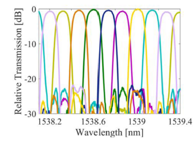
Wavelength-division multiplexing (WDM) combine and separate optical data channels whose aggregate bandwidth cannot be sampled and processed in the electrical domain. The proper function of WDM devices rely on careful interference among multiple waveguide paths. Design requires sixth-decimal-point accuracy in the effective index of waveguides, which may not be reached within open-loop fabrication tolerances. Our group has developed and employed a unique protocol for one-time post fabrication trimming of phase delays in silicon photonic circuits. The process relies on the local illumination of a photo-sensitive upper cladding layer of specialty glass, subject to closed-loop monitoring of device transmission. Using this protocol, an eight-channel WDM device with a narrow channel spacing of only 17 GHz was demonstrated. The device successfully routed data with record spectral efficiency of 2.35 Gbit/s per Hz bandwidth, in a single polarization.
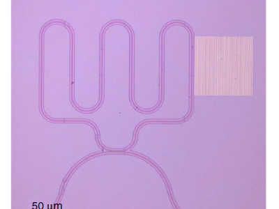
The further reduction of filters bandwidth requires prohibitively long delays, which cannot be accommodated in optical waveguides due to excessive footprint and losses. To work around this difficulty, information may be converted to the form of slow-moving surface acoustic waves (SAWs). The concept is widely employed in analog electronics for decades, and it relies on piezo-electric transduction to transfer information between electronics and acoustics. Silicon, however, is non-piezo-electric. Starting in 2019, our group has introduced a concept of SAW-photonic devices in standard silicon-on-insulator. Piezo-electric transduction and detection are replaced by the absorption of one modulated optical carrier in metal, and the photo-elastic modulation of another in a standard waveguide, respectively. Delays as long as 175 ns are acquired within 660 microns length. A similar delay in a silicon-photonic waveguide would require 17.5 meters, with losses above 1,000 dB. The concept is used in integrated, discrete-time microwave-photonic filters with up to 12 taps and bandwidths as narrow as 5 MHz. The complex magnitude of each tap may be controlled arbitrarily and independent of those of all others.
•D. Munk, M. Katzman, M. Hen, M. Priel, M. Feldberg, T. Sharabani, S. Levy, A. Bergman, nd A. Zadok, "Surface acoustic wave photonic devices in silicon on insulator," Nature Commun. 10, 4214 (2019).
• D. Munk, M. Katzman, Y. Kaganovskii, N. Inbar, A. Misra, M. Hen, M. Priel, M. Feldberg, M. Tkachev, A. Bergman, M. Vofsi, M. Rosenbluh, T. Schneider, and A. Zadok, "Eight-Channel Silicon-Photonic Wavelength Division Multiplexer With 17 GHz Spacing," IEEE J. Selected Topics Quantum Electron. 25, 8300310 (2019).